| Author |
 Topic Topic  |
|
Ampzilla
Member

133 Posts |
 Posted - 2011/04/08 : 23:35:17 Posted - 2011/04/08 : 23:35:17


|
Manual om H.Wolcott och hans konstruktioner .
Och intresset finns på andra sidan atlanten för dessa konstruktioner.
Så kommer Jag att visa hans lösningar från JBL PL-100( 1960) till föregångarn för hans Presence förstärkare(1975) i en serie artiklar .
Introduction:
Amplifier designs and information that is not readily available in cumulative
form elsewhere.
This is information collected under a long period because of the difficulties to
get the information from H.Wolcott.
He is/was a man who kept his secrets and did not put in all components in the schematics.
Henry Wolcott left some components out in the schematic drawings so they where not complete.
The reality and the schematics differ a little bit.
It was a common procedure for many manufactures.
This did it more difficult to copy a amplifier design correct without buying
one.
to be continued:
|
Edited by - Ampzilla on 2011/04/14 19:36:51 |
|
|
Bardis
Member
3348 Posts |
Posted - 2011/04/09 : 19:00:13
|
 |
Modda allt som går att modda! |
 |
|
|
Ampzilla
Member
133 Posts |
Posted - 2011/04/10 : 19:17:14
|
H.Wolcott
Då börjar informationen om denna man och hans konstruktioner som varit väldigt långt borta från gemene man/kvinna.Dessa konstruktioner blev efter det att JBL la ner PL-100 , endast tillgänglig för lab bruk. Men som till sist blev till hans Hifi Presence förstärkare under firmanamnet Wolcott Audio.
(Bild För dom som inte sett JBL:s PL-100 amplifier från 1960 2*60watt + active crossover)

Här börjar resan:

Preword:
The Tube Amplifier
Dick Ohlser
After nearly a century of evolution it is safe to say that vacuum tube circuitry has reached a state of maturity. It appears that every conceivable circuit nuance has already been investigated; no stone left unturned by a host of ingenious engineers who grew up knee-deep in vacuum tube technology. For example, even 1952 Radiotron Designer Handbook (4th Edition) already contains over 1,400 pages of information about radio receiver and audio amplifier design and application.
The resultant legacy from the golden age of audio is enormous in scope and magnitude.
It is therefore not surprising to recognize most modern high-end power amps for what they really are: recycled 50s designs with inferior output transformers. The only thing original about these products is the cosmetics. The associated advertising hype tends to deflect attention away from the essence of the circuitry and instead focuses on familiar audiophile esoterica such as wonder caps, kryptonite resistors, and magic wire. The bottom line for the consumer is often a price tag equivalent to the cost of a new car for an amp that isnt even as sophisticated (or good sounding) as a vintage Harman Kardon Citation II.
This power amplifier breaks new ground in audio electronics, but as the constructor, will tell you, its basic topology is over 40 years old,and having been used in amplifier systems he designed for JBL in 1960(PL-100). It earned him two US patents at the time. His US and foreign patent total today in instrumentation and audio design stands at an even dozen. After founding in 1961, a precision instrumentation company with sales to aerospace companies and national laboratories, he further refined the original design as a serie instrumentation amp. They was designed as a lab-grade instrument for precision calibration and testing. Over 1,100 units were sold worldwide, including six systems at the U.S. Bureau of Standards, now NIST. This new amplifier he manufacture today is the latest descendant of the original circuitry, introduced under the WA company banner in 1988. It represents a third generation version of the original design, optimized expressly to meet the needs of the high-end and professional audio markets. While each building block of the amplifier is not necessarily new, the sum total of its design elements represents an original and unique statement in the realm of hi-fi design.
I only plan to provide a few general and technical comments to give an overall feel for the the amp.
They believes that circuit topology is the primary determinant in amplifier performance. He finds traditional designs to suffer form several obvious failings resulting directly from the limitations and distortions inherent in transformer coupled output stages. Better load tolerance, greater stability, lower static distortion and output impedance, better transient behavior with lower noise, and higher power supply rejection are the stated performance objectives of the circuits.
The amps is fully balanced at all stages beyond the input stage. A major feature is the use of balanced positive (feedforward) as well as negative feedback, which allows the cancellation of the amps internal impedance. A control on the panel lets the user adjust the output impedance at frequencies below 1000 Hz from about two ohms to zero, and even about 0.5 ohm negative. Zero output impedance yields an infinite damping factor, while moving into negative territory cancels the effect of cable resistance and even some of the voice coils DC resistance.
Thus, the amp is intimately coupled to the load and is able to control transient behavior to a degree impossible with traditional designs.
A pair of 6922 dual triodes makes up the input stage. Each 6922 is configured as a White cathode follower, and the two followers are connected in parallel to create a buffer stage of high input impedance, low output impedance, and exceptionally low distortion. Negative feedback is applied to the second cathode follower from a tertiary winding in the output transformer. A pair of 6GW8 triode/pentodes makes up the second and third stages of the amp providing voltage gain and symmetrical drive signal. The pentode halves are operated as cathode followers with transistor current sources and are directly coupled to the output stage. The output stage is comprised of eight EL34 pentodes operated as pure pentodes in a conventional push-pull circuit. The output tube screen girds are actively regulated. My review samples incorporate the latest wide bandwidth output transformers with exceptionally low leakage inductance and only moderate winding capacitance. Their full power bandwidth is 20 Hz to 30 kHz, running flat out at 220 wpc into 4 ohms. These trannies feature a tertiary feedback winding (ala McIntosh#8217;s unity coupled output stage) closely coupled to the primary. This isolates the feedback loop from load fluctuations and ensures that that full error correction is provided even in the presence of highly reactive loads.
to be continued: |
Edited by - Ampzilla on 2011/04/10 19:57:22 |
|
|
|
Ampzilla
Member
133 Posts |
Posted - 2011/04/10 : 19:23:13
|
AUDIO TECHNICAL WHITE PAPER:
A FUNDIMENTALLY NEW TOPOLOGY FOR AUDIO FREQUENCY POWER AMPLIFICATION
By Henry Wolcott
Introduction :
This paper is directed to those who purchase or represent perfectionist"high end"
audio amplifiers. Our aim here is two-fold. To present a significant new technology and
to discuss that technology in the contest of high fidelity amplifier design as it has been
practiced to date. Naturally, we hope that your reading of this document will persuade
you to look favorably on our product, but we also trust you will obtain useful factual
information on significant issues in amplifier design-information that is not readily
available in cumulative form elsewhere. We attempted to present engineering
concepts in plain English insofar as possible and we hope that in some small way this paper
contributes to a wider understanding of the fundamental principles and constraints of
Audio amplifier circuit design.
Reinvigorating a Stagnant Technology
The basic design of both solid state and vacuum tube audio power amplifiers can
be said to be mature. No significant innovations in circuit topology have been developed
within the last ten years and the current art in amplifier design would appear to have
exhausted the possibilities of basic analog circuit configuration. For the perfectionist
user, this state of affairs cannot but be distressing because no extant design in the
marketplace approaches the ideal.
Our firm is introducing an amplifier topology without close precedent, the first
radically innovative design to appear in more than a decade in either the solid state or
vacuum tube categories. We believe it is demonstrably better than established topologies
across a broad range of performance parameters, in other words, better in virtually
every way.
The circuit described in this paper is certainly unique, but is new only in the sense
of being new to consumer electronics and in having been recently revised to make use of
modern component types and manufacturing processes. The basic circuit was actually
developed in the early sixties and the designer was granted two U.S. patents at that
time. Nevertheless, the topology is entirely unprecedented in high fidelity applications
In addition, represents a highly significant development in this area.
Before we discuss the specifics of the design, we would like to express a position
that needs restating in the high-end audio marketplace where we are attempting to
promote our product. We believe circuit topology is the main determinant in amplifier
performance and the preoccupations of many contemporary designers with resister
and capacitor types and even interconnect wiring is misguided and is, we think, indicative
of the general paucity of real design innovation prevailing in the high end today.
We certainly dont maintain the quality of passive components is un-important, but beyond a
certain minimum level of parts tolerance, component quality is secondary to circuit
topology in the ultimate determination of system performance. Thus we view the
common high end practice of constructing flawed circuits out of exotic capacitors and
resistors as distinctly unpromising and altogether unlikely to overcome the limitations of
such circuits or to advance the art of amplifier design in any significant way. We would
further suggest the truth of our position can easily be demonstrated in listening tests and
in bench measurements.
Why Vacuum Tubes
From the time our basic topology was developed some thirty years ago to the present,
enormous progress has been made in the design of solid state amplifiers and in
the formulation of solid state devices themselves. Due to the improvements in transistor
design, coupled with the inherently lower maintenance requirements of solid state gear,
most designers aiming to create a highly accurate as opposed to a euphonic amplifier
Circuits have opted for transistors. We have not and we would like to explain
why. Both solid state and tube amplifying circuits are highly problematic and both
present the design engineer with formidable challenges. Challenges that are well worth
examining. The fundamental design limitations facing the solid state engineer remain the
limitations of the devices themselves, resulting in many distortion mechanisms,
inherently low power bandwidth, temperature instability and hard clipping characteristics.
The fundamental limitations facing the vacuum tube designer are more various,
lying in the high output impedance of the devices and lack of complementary forms, the
disadvantageous relationship between gain and linearity, the gross frequency limitations
of the coupling transformers required at output and of course the high cost, inefficiency
and high heat output inherent in vacuum tubes themselves. Perhaps rather surprisingly,
we found the limitations of vacuum tubes to be less intractable. In other words, at this
late date, it is still possible to build a better power amplifier with the archaic vacuum tube
than with the very latest solid state devices. The following sections indicate just how we
have arrived at this conclusion.
to be cont. |
Edited by - Ampzilla on 2011/04/10 19:41:18 |
|
|
|
Ampzilla
Member
133 Posts |
Posted - 2011/04/10 : 19:43:00
|
Relationship to Prior Art
In the late fifties and early sixties when the new topology took its initial form, the
object of the design project resulting in this topology was to develop an amplifier with a
vanishing low distortion, which advanced the art of design several steps. At the time,as
a matter of interest, solid state circuitry wasnt even considered for the project. Solid
state circuits of the day were known to be prone to crossover distortion, transient
distortion and instability in the face of reactive loads. The output devices of the day
didnt lend themselves to high power applications. Instead, the project would build upon
the long established discipline of vacuum tube circuit design.
Vacuum tube power amplifier design as practiced then and as practiced now for
the most part, proceed along well worn paths. The huge majority of audio frequency
power amplifiers utilized three stage circuits consisting of a single ended input with gain,
a phase splitter, generally of the long tailed inverter type and also producing voltage gain
and a push pull, plate coupled output stage with gain as well. Sometimes, by the way of
variation, the phase splitter would constitute the first stage and the second stage would be
push-pull as well as the output and sometimes a cathode follower driver stage would be
present to provide low impedance drive to the output tubes. And there was other
refinements as well, some reflecting considerable design ingenuity, but very few of which
posed any real challenge to traditional engineering. Indeed, the only really major
departure from the past among the current art is the frequent presence of some form of
regulation in the power supply, generally by means of high voltage solid state regulators
which simply werent feasible at the time the new topology was developed.
Power amplifiers designed according to the traditional practice have numerous,
fairly serious [performance limitations, including rather high static distortion, often over
a percent and never less than a tenth of a percent, high output impedance and generally
rather narrow full power bandwidths that barely span the audible spectrum. Signal to
noise ratios are poor in relationship to solid state equipment and the circuits are prone to
hum and ground loops. On the other hand, such distortions as they are produced, tend
toward the euphonic and for reasons not fully understood, traditional tube topologies
appear to render ambience more convincingly.
When such circuits are analyzed carefully, it will be seen that most of the obvious failings arise from the behavior of the transformer coupled output stages.
Typically these use pentodes or beam power terrodes which tend to generate fairly high
distortion and much of that, higher order harmonics! Furthermore, such tubes have
extremely high output impedance and are difficult to couple to the loudspeaker loads even with matching transformers.
The problems inherent in the traditional designs were well known at the time the
new topology appeared and had been addressed in one major design variant that is, in its
various manifestations, invariably distinguished by the use of a characteristic unity
coupled output stage. Originally patented by McIntosh Corporation in the forties and
subsequently used in their own products as well as those of Krohn-heit and Electrovoice,
among others, the unity-coupled output is a partial cathode follower with no gain at all,
resulting in nearly one hundred percent feedback around the output stage, nearly perfect
balance between both halves of the transformers, high efficiency, negligible notch
distortion, low output impedance and wide full power bandwidth. (A cathode follower,
for those of you who may have forgotten tube fundamentals, is a topology where the
output is taken from the circuit of the negative element of the tube, the cathode, thus
bypassing the internal resistance of the tube; cathode followers provide current gain but
no voltage gain and are normally used for impedance matching.) Properly designed unity
coupled amplifiers also produced comparatively low distortions, sometimes less than a
tenth of a percent at full power.
The unity coupled output stage poses considerable manufacturing difficulties due
to the complex output transformer it demands, but there can be no question that it
represented a considerable advance in the art. We always regard these designers as
worthy competitors, though we regularly outperformed them in demanding
instrumentation and industrial applications.
Our own topology represents the second major attempt to improve upon the
traditional single-ended three stage vacuum tube power amplifier. It also represents the
last significant new design using vacuum tubes throughout the signal circuitry.
to be continued |
Edited by - Ampzilla on 2011/04/10 19:58:41 |
|
|
|
Ampzilla
Member
133 Posts |
Posted - 2011/04/10 : 19:52:08
|
ANATOMY OF A BREAKTHROUGH
Though somewhat more complex than the unity coupled types, our circuit offers
lower static distortion, lower output impedance and consequently better damping, greater
stability, much better load tolerance, equal or better bandwidth, better transient behavior,
faster recovery times, lower noise and higher power supply rejection.
To achieve such superior performance, the circuit incorporates the following
unique design elements.
1. It uses a form of feed-forward which effectively swamps the distortion of the
output stage.
2. It uses a highly linear, non-inverting symmetrical gain stage combining very
High gain almost unmeasurable open loop distortion.
Within this stage, the two halves of the circuit are operated in an antiphase
Relationship without inversion; that is, one tube produces a positive output with a
negative input, while the other produces a negative output with a negative input.
Symmetrical operation of paired vacuum tubes within a gain stage will theoretically
result in similar common mode characteristics to solid state complementary circuits and
were for years the philosophers stone of vacuum tube circuit designers. The long
sought after design breakthrough defied the efforts of the best engineers. Such operation
has never been deemed practical with conventional tube types and our success in
accomplishing it removes one of the most fundamental limitations of vacuum tube
circuits sui genres.
The circuit is fully balanced at all stages beyond the input stage and is dual
differential in the main gain stage, that is, each half of the symmetrical circuit is itself
differential.The unique balanced topology of the amplifier ensures that power supply
ripple and fluctuations are common mode and will not be amplified. Such balance is
achieved through operation of tubes as complementary devices, cross coupling of the
circuit at the main gain stage, application of feedback to both halves of the circuit and by
the use of a perfectly balanced output transformer.
The circuit uses balanced negative and positive feedback around both of its
halves, other amplifiers have featured balanced feedback but never used within a
symmetrical circuit topology. The circuit uses parallel White cathode followers at input
for the virtual elimination of distortion at that stage, as well as greatly reduced internal
resistance and an unparalleled reduction of the thermal noise inherent in tube operation.
The circuit incorporates an output transformer of unique design which effectively
prevents adverse load interaction with the signal circuitry and contributes negligible
distortion of its own. When driven from a constant voltage source as is the case
with our output circuit at higher frequencies, this transformer provides flat frequency
response out to beyond 30-kHz.
The circuit is unusual though not absolutely unique in its use of constant current
sourcing by means of active devices and both active and passive voltage regulation, the
former by means of solid state amplifiers and the latter by means of zener diodes, which
is capacitor bypassed for the lowest noise. The circuit is also unusual in offering an
impedance adjustment at output permitting zero and negative output impedances.
to be cont. |
Edited by - Ampzilla on 2011/04/10 19:58:11 |
|
|
|
Ampzilla
Member
133 Posts |
Posted - 2011/04/11 : 13:01:22
|
Signal Circuitry Specifics
The rest of this paper is devoted to a detailed analysis of the schematic from input
to output. The circuit consists of four stages, only one of which contributes appreciable
gain. The first and third stages are essentially buffers, while the gain of the output stage is
effectively swamped by the gain of the second stage which itself constitutes the main
gain stage. A total of twelve tubes and sixteen sections are utilized. Two 6DJ8 dual
triodes are used at input, a pair of 6GW8 combination triode/pentodes comprise the
second and third stages and eight EL34 power pentodes are used at output.
First Stage - Input Stage
The input stage of the circuit utilizes a topology known as a White cathode
follower consisting of a conventional cathode follower sourcing current from the plate of
a driven bottom tube. What differentiates the White cathode follower from a simple
cathode follower with a tube constant current source is the connection between the plate
of the cathode follower and the grid of the bottom tube, which brings the current source
under feedback control and provides for a very constant impedance when sinking or
sourcing current. Theoretically the impedance of the lower tube approaches zero, actually
equaling a few ohms.
The White cathode follower which is a high input impedance, low output
impedance, virtually distortionless circuit which properly loads the line level component
driving the amplifier while providing nearly ideal low impedance drive for the critical
either dont gain stage to follow. The White cathode follower is not our invention, but it
has seen little use in consumer audio in spite of its manifest advantages.
We may speculate that most manufacturers understand the topology or dont wish
to incur the expense of an additional tube. Parallel with the input is another White
cathode follower, which accepts a negative feedback signal from a tertiary winding from
the output transformer. The purpose of sending the feedback through an active buffer
stage is to cancel out any noise engendered by the signal input stage (how this is
accomplished is explained below). The extremely low noise of our amplifier is largely
due to the presence of mirror image circuits for feedback and input. Incidentally, both
circuits use actively regulated, positive and negative supplies.
|
Edited by - Ampzilla on 2011/04/11 13:02:45 |
|
|
|
Ampzilla
Member
133 Posts |
Posted - 2011/04/13 : 12:11:55
|
Second Stage - Linear Gain Stage
The second stage of the amplifier consists of the triode halves of a pair of 6GW8
combination triode/pentode tubes operated as a true complementary symmetry pair in a
manner that is somewhat suggestive of solid state topologies employing NPN and PNP
transistors. Operation is as follows:
Each half of the complementary circuit is driven in push-pull fashion by the single
ended output with the White cathode follower without the necessity of a phase inverter.
The output of the bottom White cathode follower drives both the cathode of the bottom
triode section and the grid of the top triode section, producing antiphase outputs at the
plates of the two triodes.
Normally Driving a tubes cathode produces little or no signal gain, a fact which
encouraged De Forrest and others to experiment with signal grids in the first place.
However, if the plate of the tube sees an effectively infinite impedance, then gain
can be achieved by bootstrapping, a fact which is well known, though no one previously
seems to have recognized the scope that bootstrapping provides for constructing
symmetrical circuits using vacuum tubes. Moreover, cathode drive may be further
facilitated by driving the cathode from an ultra-low impedance source such as a White
cathode follower.
We could perhaps mention here, we cannot claim absolute priority in the use of
vacuum tubes in a non-inventing mode, nor even in the use of crosscoupled tube circuits
with opposite grid and cathode drive and separate mirror image cathode follower inputs
for signal and negative feedback. Unfortunately, when crosscoupling is attempted absent
an ultra-low impedance source and an infinite plate load as has been the case in the prior
art, the symmetry of the resulting circuit is not very good, nor is its open loop linearity.
To be sure, other means have been devised to operate tubes in a non-inverting mode to
approximate the characteristics of double ended circuits using different sex devices, most
notably, the totem pole circuit used in many OTLs. Here cathode followers are
combined with plate followers in a series connection to ground and the two tubes are
driven in antiphase with the two tubes loading one another. However, such circuits can
scarcely be considered symmetrical either and their open loop linearity is extremely poor.
Such parallels notwithstanding, no one, to our knowledge, has previously published a
circuit for a non-inverting, truly balanced main gain stage driven by a single ended input.
.We would also mention that within our topology, cathode drive provides yet
another advantage. When the tube whose cathode is driven takes it#8217;s input from a cathode
follower, an almost complete cancellation of distortion occurs as a result of the antiphase
relationship of the two tubes, this in turn sharply lowers the inherent distortion of the gain
stage prior to the application of feedback.
To return to our description of the second stage, the feedback from the top White
follower of the input stage drives the cathode of the top gain triode and the grid of the
bottom gain triode. The feedback loop is split in effect and thus the negative feedback
itself enters both halves of the symmetrical circuit. The two resulting legs of the
feedback loop bear an antiphase relationship with one another and thus unlike a single
ended feedback loop, this balanced pair cannot create multiples of residual harmonic
distortion because, the push-pull relationship of the feedback paths themselves will buck
out such multiples.
The feedback signal in either half of the circuit functions somewhat differently
than negative feedback in a more conventional circuit in that the feedback signal bears a
differential relationship with the main audio signal. Furthermore, the feedback is
negative only by virtue of its driving the other half of the differential. It is not phase
reversed by a capacitor as in conventional circuits and thus it is not bandwidth limited.
The feedback is very nearly as fast as the signal itself and so slew limiting or transient
distortion at audio frequencies due to feedback cannot occur. Furthermore, again due to
the differential relationship, the actual gain of the tube is a difference signal and the
distortion products in both the audio signal and the feedback signal are common mode
and thus cannot be amplified. Thus the effect of the feedback in the gain stage is a
virtually one hundred percent reduction of distortion. Any residual distortion not
eliminated by the negative feedback loops will be present in equal measure in both halves
of the circuit and thus will be bucked out at the output stage. The cross-coupled negative
feedback loops become in effect a highly linear push-pull error amplifier.
The crosscoupling of negative feedback and signal circuits has a parallel in the
use of positive feedback in the new topology. Positive feedback taken from the cathode
circuits of the third stage is also sent to both halves of the voltage swinger circuit with the
positive feedback loop from the top pentode section driving the cathode of the top triode
section and the grid of the bottom triode section and the positive feedback from cathode
of the bottom pentode driving the cathode of the bottom gain triode and grid of the top
gain triode.
The effects of this arrangement are several. First, the gain of the triode gain stage
rises toward infinity before the application of negative feedback, which essentially
eliminates the imbalance between the cathode and grid driven tubes and which instead
makes for almost perfectly symmetrical drive. When this #8220;infinite gain is subsequently
reduced by the application of negative feedback, the noise floor of the circuit drops
dramatically. Second, the distortions of the circuit in theory becomes infinitely small
because enormous gain necessarily results in enormous voltage feedback as well,
(Obviously the gain and feedback must have some finite value for stability to be
preserved).
Third, perhaps most interestingly, the odd order distortion products of the gain
stage, small though they may be, are distributed to both halves of the circuit in an
antiphase relationship so that they too are bucked out when the two halves of the circuit
are summed in the output transformer. Conventional push-pull circuits only eliminate
even order distortions, but this new topology eliminates both types. Finally, the positive
feedback provides the means of swamping the distortion of the output circuit simply
because of the enormous disproportion of gain and voltage swing between the two stages.
The voltages seen at the output terminals of the amplifier are essentially those generated
at the second stage.
Now it might be objected that an infinite gain/infinite feedback circuit such as we
have described would suffer from many of the same liabilities as the ill regarded high
gain solid state op amps, namely marginal high frequency stability and very low open
loop bandwidth. Indeed common engineering theory dictates that in any feedback system
the negative feedback will be phase shifted to positive feedback as reactive elements in
the circuit begin to exert filtering functions with increasing frequency. This being the
case, in order to avoid instability in the presence of degenerative feedback, the circuits
gain must fall to unity at the frequency where the phase of the output has undergone one
hundred eighty degrees of shift. Obviously in a circuit of infinite gain, compensation
would have to begin at DC and the circuit would have no open loop bandwidth
whatsoever, while in a circuit approaching infinite gain i.e.,with a gain in the millions,
the output would have to be rolled off beginning at a break point below 100-Hz, which is
exactly the region where high frequency compensating filters are located in commonly
uses op amps.
However, as a matter of fact, we dont use any compensating filters at all in the
usual sense and the open loop bandwidth of our main gain circuit extends out into the
megahertz. We are not claiming any logical impossibilities here, as indeed would be the
case if we were dealing with a conventional topology. What we do to prevent oscillation
while preserving open loop bandwidth is to include another pair of negative feedback
loops, one for each half of the circuit, extending from the primary of the transformer to
the summing junctions and contoured so as to come into play only at ultrasonic
frequencies. These nested loops progressively reduce both the positive feedback and the
negative feedback coming from
the tertiary winding, so that at high frequencies the amplifier becomes a low gain, low
feedback circuit whose output does not roll off progressively simply because open loop
gain and degenerative feedback diminish by exactly the same proportion. In other words,
at high frequencies the gain stage comes to resemble an ordinary low mu feedback triode
circuit extension. Or put it still another way, one derives all of the benefits of ultra-high
feedback at audio frequencies while retaining extended open loop bandwidth and
reasonably low distortion far into ultrasonics.
There is yet another benefit to this scheme, namely the effect that it has on
clipping. Typical high gain, high feedback amps misbehave badly when overloaded.
Clipping effectively disengages the negative feedback loop because the voltage at the
output no longer bears a linear relationship to the input so progressively less feedback is
available. That in turn increases the gain of the circuit so the gain device is pushed right
up against its voltage rails for abrupt, severe, flat-topped clipping. That doesnt happen
with our design because the positive feedback loop, which engenders most of the gain in
the circuit, is progressively decoupled as well as the negative feedback loop, so the circuit
doesnt take off in the presence of overload. Because clipping will occur only in the
output stage under normal circumstances, the basic disproportion in gain between main
voltage swinger and output will still be present far into overload, though diminished and
thus the behavior of the amplifier under conditions of hard clip will actually be better
than a typical low feedback, push-pull vacuum tube amplifier.
As indicated earlier, this is not the first amplifier to employ balanced positive and
negative feedback in an infinite gain/infinite feedback relationship, but it is the first
practical implementation of the concept. All earlier embodiments were single ended and
tended to oscillate in the presence of minor offsets. Moreover, clipping was generally
accompanied by very violent oscillation as the negative feedback loop ceased to stabilize
the gain and the positive feedback loop was thereby allowed to increase the gain of the
amplifier to the point of overload. Finally, in prior art involving balanced feedback, the
negative loop was always taken from the secondary, which because it was in series with
the speaker load impedance, would impose filtering effects upon the feedback signal
which in turn would invite oscillation at certain frequencies. In the new design, offsets
do not occur. Under clipping conditions the gain of the second stage progressively
diminishes so that the reduction of negative feedback is exactly matched by the reduction
in gain. Because the main feedback loop is taken from a tertiary winding, the feedback
signal itself is isolated from the speaker load. For all of these reasons, the amplifier can
have exceedingly high negative feedback while still exhibiting absolute stability. In fact,
better stability than that afforded by any low feedback design.
To conclude our discussion of voltage amplification in the circuit, the second
stage is provided with passive plate regulation via a zener diode with bypass capacitors
for maximum linearity. Because of the symmetrical nature of the circuit, power supply
rejection is extremely high to begin with. Regulation only improves a fundamentally
stable circuit. |
Edited by - Ampzilla on 2011/04/13 14:26:34 |
|
|
|
Ampzilla
Member
133 Posts |
Posted - 2011/04/13 : 14:28:55
|
Third Stage Buffer and Bootstrap
The third stage consists of the pentode halves of the pair of 6GW8s operated as
cathode followers. This stage has two basic functions in the circuit, providing the output
stage with a low impedance drive and effecting a bootstrap loading for the preceding
stage. The cathode follower is essentially unity gain and so when its output is placed
across the plate resistor, the plate of the triode sees no change in the voltage of the plate
circuit. The bootstrap circuit forms an active load for the plate of the triode and presents
it with and effectively infinite load impedance. The effects of this scheme are three fold:
the open loop linearity of an already highly linear device is improved enormously, indeed
open loop distortion for single ended operation of this circuit is just slightly over a
hundredth of a percent maximum below clipping. Secondly, the gain of the triode is
made to equal the mu of the tube. Finally, bootstrapping ensures the gain of the tube will
remain constant as the tube ages.
The high degree of linearity inherent in the bootstrapped triode configuration is
important because positive feedback has the effect of multiplying any distortion in the
circuit. The circuit has to be made virtually distortionless through optimal loading before
positive feedback can be allowed to increase the gain.
The output of the pentode cathode follower is direct coupled to the output stage
and constant current sourced by a pair of transistors forming a current mirror. The grid
circuit of the output tubes is connected to a digitally controlled automatic bias circuit
which checks and resets individual tube biases at turn-on and then is disengaged from the
signal path. |
Edited by - Ampzilla on 2011/04/13 14:29:24 |
|
|
|
Ampzilla
Member
133 Posts |
Posted - 2011/04/13 : 14:33:17
|
Fourth Stage - Output Circuit and Output Transformer
The output stage is a reasonably conventional push-pull plate coupled circuit
operated in a pure pentode mode. The screens of the tubes are actively regulated, a fairly
common practice in pentode or beam tetrode outputs.
Nevertheless, the behavior of the output stage is far from conventional due to the
circuitry which has preceded it and the rather unusual output transformer that follows it.
The positive feedback, as we have seen, virtually swamps the gain of the output
stage and buries most of the distortion. It does so by enormously increasing the value of
the negative feedback so that the voltages representing antiphase components may exceed
the value of the distortion itself, in other words, the distortion of the output stage is
completely obliterated in theory. Any possible residual will appear on both sides of
the output transformer and will be bucked out.
A secondary pair of positive feedback circuits senses output current via a resistor
across the ground termination of the secondary and provides the voltage to overcome the
output impedance of the secondary so that the amplifier has a virtual zero impedance and
thus a theoretically infinite damping factor. Not only does a zero impedance vastly
improve woofer control, but it also prevents the development of distortions in the
output circuit due to back e.m.f. There#8217;s simply no resistance across which the back of
e.m.f. can develop a voltage and thus no way a distortion can arise. As we#8217;ve seen, the
zero output impedance also ensures flat response into reactive or low impedance speaker
loads, thus improving the stability of the amplifier.
A further rationale for using a positive current feedback loop is the scope it
affords the designer for overcoming the reactive losses of the transformer and extending
the bandwidth of the output stage without recourse to either an equalization stage or
potentially destabilizing negative feedback around the secondary, the latter being the
usual practice. Our amplifier uses a contour circuit in the positive current feedback loops
that applies more positive feedback at high frequencies to extend frequency response , but
does not interact with the speaker load to create instability problems and which actually
improves the high frequency phase behavior of the transformer. Our amplifier will pass
an excellent square wave at 10 kHz, a feat we have never seen duplicated in any
transformer coupled vacuum tube amplifier. No surprisingly, high frequency
reproduction is exceptionally smooth, uncolored and extended. |
|
|
|
Ampzilla
Member
133 Posts |
Posted - 2011/04/13 : 14:39:53
|
The Transformer
The design of the output transformer is proprietary and cannot be disclosed in
detail. The transformer itself exhibits probably the widest bandwidth and lowest
distortion of an plate coupled transformer for an amplifier of this power class. While
details of construction will not be touched upon, we can discuss a few general aspects of
the design which are especially salient to the operation of the total circuit.
The transformer utilizes a tertiary feedback winding for the main negative
feedback loop extending back to the top White cathode follower. The tertiary winding is
very closely coupled to the primary and ensures that any distortions engendered by the
primary or the core will be canceled by the loop. At the same time, the feedback loop is
isolated from load fluctuations and cannot be disturbed by filtering effects of complex
load impedance. Additionally the isolation afforded by a tertiary winding allows the
feedback loop to provide full error corrections even in the presence of highly reactive
loads so that distortion does not increase with load reactance, a unique benefit of the
design.because the feedback value is defined by the winding ratio of the transformer
rather than by a resistor value as in conventional design. The tertiary winding also
ensures the bandwidth over which the feedback operates, far exceeds the full power
bandwidth of the amplifier, thus the feedback need not be rolled off by a low pass filter to
prevent oscillation. The feedback loop is very nearly as fast as the circuitry it surrounds
and the loop itself encloses only one significant filter pole due to the presence of only one
real gain stage. So in essence, the main feedback loop is a local loop.
As indicated in an earlier section, we also take negative feedback from the
primary, though only at high frequencies. This second negative feedback loop serves to
stabilize the entire circuit in the presence of intense high frequency transients, but it also
provides another benefit in the context of our unique transformer design, namely the
extension of high frequency response beyond what has been possible with plate coupled
vacuum tube designs.
In audio frequency transformers, high frequency response is limited by two
factors, the leakage inductance appearing across the secondary and the shunt capacitance
between the coils of the primary. Normally attempting to minimize these two reactive
properties involves design contradictions, so that a transformer with well controlled
capacitance will tend to suffer from excessive leakage inductance and vice versa. While
we have not resolved this fundamental contradiction entirely, we have succeeded in
designing a transformer with extremely low leakage inductance and only moderate
capacitance.We therefore have a transformer that provides us with full power output from
20-Hz to nearly 20-kHz, which is altogether extraordinary at the power levels at which
we operate.
Here we feel compelled to point out that the esoteric wing of the audio industry is
simply awash with misleading specifications regarding transformer bandwidth and a
purchaser comparing performance would do well to understand transformer design
principles and bandwidth specifications thoroughly.
Practically all transformer coupled tube amps take feedback from either the
primary or the secondary, sometimes both. When the transformer is included in the
feedback loop, the low-level bandwidth will increase, often dramatically, though the full
power bandwidth will not increase at all! The feedback loop will in effect tell the
amplifier to increase its gain when the transformer response begins to droop but, the
transformers reactance will remain the same and will impose absolute limits on the
amplifiers power delivery. Not surprisingly, most manufacturers list bandwidth, (actual
level usually not specified) and not full power bandwidth when characterizing the
amplifiers frequency response. Thus claims of 100-kHz full power bandwidth, so
regrettably common nowadays, should be regarded with utmost suspicion. Such
performance may be possible with a pure cathode follower output stage working into an
autotransformer, but not with any more conventional output topology. We have done
exhaustive tests on classic tube designs from the sixties from Marantz, Harman-Kardon,
Dynco and McIntosh, all of which had transformers that were far superior to the current
norm and we have never found full power bandwidth in excess of 80-kHz even in very
low powered units. The fundamental behavior of inductors simply works against
appreciably greater full power bandwidths. However, it is entirely possible, though not
easy, to obtain low power response out into hundreds of kilohertz and this is precisely
what we have been able to accomplish with our design.
If a transformer with very low inductance, but moderate capacitance is driven by
low impedance source, namely an output stage with feedback taken from the primary, the
effect of the capacitance will be nullified and inductance alone will limit high frequency
response. Naturally, the feedback eats up gain, while capacitance reduces efficiency, so,
full power output is not going to be possible at frequencies beyond 50-kHz, but the small
signal linearity of the amplifier will be much extended and in our case the 6-db down
point is well over 70-kHz, while 10-kHz square wave reproduction is almost perfect with
no rounding or ringing.
Finally, we should mention that up to the secondary of the transformer, the new
topology may be said to be virtually distortionless. The secondary is out of the loop and
appears to be the source of the small amount of measurable distortion remaining in the
amplifiers output. We balance the transformer very carefully to minimize that distortion.
|
Edited by - Ampzilla on 2011/04/13 14:41:47 |
|
|
|
Ampzilla
Member
133 Posts |
Posted - 2011/04/14 : 19:35:43
|
The Topology in Context
Nothing is new under the sun says the Book of Ecclesiastes. Who are we to
disagree with Holy Writ? Most aspects of the new topology have been foreshadowed,
but the interrelationship between circuit elements is unique.
The use of a combination of positive and negative feedback, termed balanced
feedback by some, has certainly been anticipated by earlier designers. Prior efforts
along this line were never very successful. Previous balanced feedback
topologies were all single ended and, as we have seen, positive feedback within a single
ended circuit is highly destabilizing since power supply fluctuations can instantaneously
alter gain enough to send the circuit in oscillation. Moreover, all such earlier efforts
utilized an op amp approach of raising gain with positive feedback simply to permit more
negative feedback to be applied. We were the first to use positive feedback to crosscouple
and balance a gain circuit.
Finally we would like to say a word concerning our use of high values of
negative feedback, its precedents in the field of vacuum tube electronics and its
relationship to the high feedback designs of mainstream solid state designers.
High feedback is difficult to implement in conventional tube amplification
circuits. The triode gain stages which prevail in audio circuits have low amplification
factors and won#8217;t support much feedback unless they are cascaded, which in itself tends
to limit the values of overall feedback applied wideband, this due to the multiplication of
filter poles. Moreover, the output transformers tend to shift the phase of feedback
radically when feedback is taken from the secondary. Of course one can take the loop
from the primary but, then the distortion of the transformer is not corrected and so
relatively little is accomplished. Our method, using a single gain stage, a tertiary winding
and a second high frequency short loop, is the only way to ensure both stability and ultra
low distortion in a high feedback transformer coupled design.
Output transformerless (OTL) tube amps, which, incidentally, were mere
couriosities when we were developing the new topology, can and usually do operate with
high values of global feedback since the basic linearity of the circuits is so poor when
operated in open loop. Here we see a few analogies with our own work. Rather we see
a virtual anticipation of bad design practice in solid state-start with a dirty high gain
circuit and try to tame it with a heavy dose of feedback. We will add parenthetically
that the current promotion of OTL designs in the in the high end market place is based
very largely on marketing considerations. The concept has almost no real engineering
validity!
Which brings us to the subject of the solid state norm#8230;#8230;#8230;
Transistors generally are relatively nonlinear narrowband devices with numerous
modes for generating distortion. Feedback of one sort or another is absolutely necessary
to operate transistors in high fidelity audio circuits. Most transistorized amps made
today use massive amounts of global negative feedback, sometimes as much as 100-db.
To get the gain to use that much feedback, the designer cascades several gain stages and
resorts to active loads such as current mirror-tactics which no one would use in designing
for open loop linearity. Such high gain circuits generally exhibit very poor open loop
performance, with high values of distortion and very limited bandwidth and as a
consequence, amplifiers of this sort almost invariably display poor transient performance
even while maintaining very low static distortion. The typical op amp IC type of solid
state design has unfortunately given high feedback a very bad reputation among
discriminating listeners, so much so that we announce the fact that ours is a high
feedback design with some trepidation.
But in our own defense we will point out the feedback arrangement which we
employ has none of the usual side effects. It doesn#8217;t change the harmonic order by
multiplying high harmonics while eliminating second and third. And, it doesn#8217;t
exacerbate transient distortion. What it does do is to eliminate all residual distortion
from an already highly linear circuit and to provide for constant voltage characteristics at
output. All the benefits and none of the detriments!
Summary
The new topology reduces static distortion to a level on a par with high feedback
solid state equipment while avoiding transient distortion and complex IM. Stability and
performance into complex loads are unparalleled and signal to noise is equivalent to that
of well designed solid state equipment. Overall performance sets a new level for the
product category. Except for the output transformers, common component parts are
utilized throughout.
In its overall excellence, the new topology represents a major advance in sound
Reproduction and we believe based on outside listening evaluations, the new topology
Will find wide acceptance among sophisticated consumers.

END part 1
Hoppas detta gav en liten inblick och hyfsad information om HW och hans konstruktion.
Det som kommer sen är tekniska beskrivningar på olika förstärkare som han gjort.Från JBL:s PL-100.
to be continued: |
Edited by - Ampzilla on 2011/04/14 19:37:59 |
|
|
|
Ampzilla
Member
133 Posts |
Posted - 2011/04/26 : 22:49:50
|
Nu är jag tillbaka från en liten 8 dagars tur till Rom. Där jag laddat och fått lite nya ideer och energi.
Här kommer fortsättningen om Wolcott:s förstärkarkonstruktioner
(Med reservation för småfel i texten )
Detta är teknisk beskrivning från hans patentbeskrivning
(bilder kommer i slutet)
Jag börjar med JBL PL-100
WIDE RANGE HIGH FIDELITY BALANCED AMPLIFIER
1960 ( us pat. 003111 630)
H.Wolcott
The invention relates to electrical amplifiers and particularly to amplifiers of audio frequencies in which high fidelity and wide frequency band are obtained by employing balanced feedback.
While the prior art has employed negative feedback in audio frequency amplifiers, such feedback has usually encompassed the whole amplifier; from the input to the secondary of the output transformer. With theoretically perfect components, particularly an output transformer devoid of phase shift, this arrangement gives theoretically perfect results. However, in practice, the phase shift through the transformer at high frequencies precludes the effective use of such feedback. Often, it is necessary to reduce the open loop gain and therefore the feedback at high frequencies to a point where reasonable stability can be obtained. When this point is reached, usually very little feedback remains in the circuit and the distortionreducing benefits thereof tend to be lost.
The art has known of local positive feedback and its advantages of zero output impedance and the fact that distortion in the output stage does not enter the signal output of the system. However, such feedback has seldom been used in practice because there is a tendency to oscillation at either or both of the extremes of the frequency spectrurn and to introduce power supply hum and other residuals into the signal output.
I have been able to produce an amplifier of greatly improved performance by departing from the practices of the prior art in significant new ways.
Rather than obtaining negative feedback over the whole amplifier circuit they connect the feedback circuit to the primary of the output transformer. In this way they avoid the difficulties previously mentioned and also those caused by variation of impedance and phase of the loudspeaker or similar load as a function of frequency. It is not difficult to supply a relatively low distortion output transformer, since with the substantially zero output impedance of my positive feedback arrangement the magnetizing current distortion of the transformer can not enter the output signal. No matter what might be the magnitude of this current, the zero impedance does not allow a voltage to be built up.
This have been able to eliminate the hum and residual difficulties of positive feedback and to accomplish desirable refinements in negative feedback by providing balanced feedback circuits and a summing circuit on each side of the amplifier in which the positive and the negative feedbacks are suitably combined. This results in a new amplifier structure, having substantially all of the advantages of such combined feedbacks and none of the disadvantages, as will be detailed below.
In an alternate embodiment they employ a tertiary winding and upon the output transformer for the feedback connection, which winding is closely coupled to the primary and loosely coupled to the secondary of the transformer. In a further alternate embodiment they provide a power transistor output stage. This is adapted to drive a low impedance load directly, without the use of an output transformer.
An object of this invention is to provide a high fidelity amplifier of excellent performance characteristics and of extreme stability of operation.
Another object is to provide a novel compound balanced feedback circuit.
Another object is to employ local positive feedback in a balanced manner that prevents the introduction of power supply hum and other residuals into the signal channel.
Another object is to provide a precision amplifier suited to driving galvanometer recorders, shake tables, ultrasonic devices, servo systerns, or to constitute a variable frequency power source of low impedance having a range from the subaudible through ultrasonic frequencies.
Another object is to provide an amplifier adapted for plural kinds of input connections.
Another object is to provide an amplifier capable of driving loads having power factors from zero to one, leading or lagging.
Another object is to provide an amplifier of extremely low distortion, particularly the the extremes of the frequency range of operation.
Another object is to provide an amplifier having an output circuit that may or may not be grounded.
Other objects will become apparent upon reading the following detailed specification and upon examining the accompanying drawings, in which are set forth by way of illustration and example certain embodiments of my invention.
Fig. 1 is a simplified diagram having to do with positive feedback,

Fig. 2 is a complete schematic diagram of a typical embodiment of my invention,
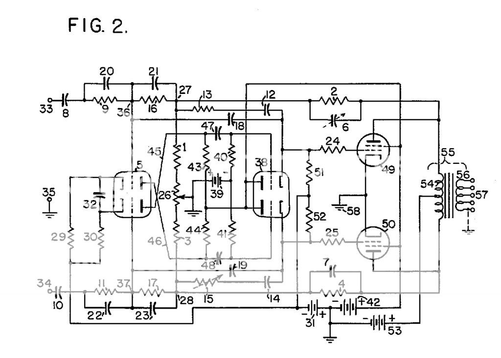
Fig. 3 is a schematic diagram of an alternate embodiment, showing a bifiliar tertiary winding on the output transformer for feedback purposes,

FIG. 4 is a fragmentary schematic diagram of the same, showing a grounded tertiary winding on the output transformer for feedback purposes,

Fig. 5 is a schematic diagram of another alternate embodiment, in which power transistors are employed in an emitter-follower configuration.

to be cont. |
Edited by - Ampzilla on 2011/04/27 22:08:35 |
|
|
|
Ampzilla
Member
133 Posts |
Posted - 2011/04/26 : 22:52:21
|
Fig. 6 is a fragmentary schematic diagram of the same, showing power transistors employed in a common-emitter configuration,

and
Fig. 7 is a graph showing the reduction of harmonic distortion as a function of circuit unbalance for my embodiment of Fig. 2.

Referring to Fig. 2, local positive feedback is applied around the first two stages of the amplifier and overall negative feedback is provided by two networks connected between each end of the primary of the output transformer and the corresponding out-of-phase grid of the input stage.
The operation of this configuration will be explained by reference to the simplified block diagram of Fig. 1.
In Fig.1, A1 and A2 represent two amplifiers in cascade; i.e. a pre-amplifying stage and an output stage.
The amplification of each is likewise identified as A1 and A2,
respectively. A portion, B1V1, of the output signal V1 of amplifier A1 is fed back to the input of A1, and a portion B2V0 of the output signal V0 of amplifler A2 is likewise fed back to the input of amplifier A1. If V1 is the signal to be amplifled, we may write, quite generably:
V1=A1(V1+B1V,+B2V0) (1)
and
V0=A2V1 (2)
Forming the ratio V0/VI by rearranging Equation 1 to be explicit in VI (rather than in V1), multiplying both numerators and denominators by A1/V1 and substituting A2V1 for V0 (from Equation 2) in the denominator of the ratio, the expression for the ampliflcation is obtained.
Accordingly, the overall amplification, A, is:
A=V0 / VI = A1*A2 / 1-A1*B2-A1*A2*B2 =A1*A2 / N
where
N=1-A1B1-A1A2B2 (4)
The total distortion, D, is given by:
D=(1/N)*D1 + (1-A1B1)*D2 / N+ (1-A1B1)* D1D2 / N (5)
where D1 and D2 are, respectively, the distortions of the individual amplifiers involved.
When A1B1 is made unity a very special situation arises.
The total amplification is equal to 1/B2 and is, therefore, independent of A2. The output impedance is zero. The distortion of amplifier A2 does not contribute at all to the total distortion.
The total distortion is thus entirely due to the first amplifier A1 and is numerically equal to its distortion in the absence of feedback times the quantity 1/A1A2B2. Since the value of this quantity can be considerably greater than one, the resulting distortion can be appreciably less than that of the first stage alone. This is a particularly advantageous situation in the case of power amplifiers, where the output stage A2 contains the relatively high distortion-producing output tube and transformer elements. Since with local positive feedhack the output stage distortion does not enter, the variation of characteristics or equality of a pair of output tubes is not of importance. Thus, a dynamic balance control or pairs of matched tubes are not required.
In spite of the benefits indicated by theory, local positive feedback has not enjoyed acceptance in commercial equipment. This has been because of the difficulty of maintaining stability in practical circuits. There has been a tendency toward oscillation at either or both of the high and low frequency extremes of the passed band. Also, the amplifier has been sensitive to power supply ripple and to variations of supply voltages caused by line voltage transients or varying demand on the power supply.
We have eliminated these disadvantages by providing a fully halanced push-pull amplifier with balanced feedback circuitry. This configuration results in the noise and variations mentioned appearing as common mode variations, and these are greatly attenuated in an amplifier of this kind. The tendency toward oscillation or instability has been eliminated by placing the output transformer outside of the feedback loop and by optimizing the response of each of the two cascaded stages.
Amplifier stabiity is recognized by the attainment of critical damping. This I have achieved by limiting the feedback loop to two high and two low frequency time constants. (RC or LR minimum phase shift networks.) This limitation restricts an A.C. coupled amplifier to two stages (without phase compensation). At low frequencies each pair of coupling capacitors and each transformer count as one time constant.
A further requirement for critical damping is that the time constant be staggered; i.e., have different values.
The staggering ratio required is determined by the amount of feedhack used. For 20 db of feedback the ratio is greater than 40 to 1. In the low frequency range this usually means that the frequency where roll-off begins due to the coupling capacitors must be less than 1/40 the frequency where roll-off begins due to the output trans- former. The frequency at which roll-off begins is not constant for the usual output transformer because of variation of the primary inductance. This is caused by variation of the permeability of the core, which is a complex function of the signal level and of the unbalance of plate currents in the output stage.
to be cont. |
Edited by - Ampzilla on 2011/04/27 22:30:50 |
|
|
|
Ampzilla
Member
133 Posts |
Posted - 2011/04/26 : 22:55:10
|
At high frequencies the usual output transformer presents further difficulties. It alone may account for two or three time constants, depending upon the conditions of use. When driven from a relatively high impedance source and terminated in a resistance it displays the characteristics of an LCR network; having two time constants and 180° maximum phase shift. When terminated in a capacitative load; such as a line matching transformer, electrostatic loudspeaker or a long transmission line, it displays the charactenistics of a PI network; i.e. three time constants and 270° maximum phase shift.
It is seen that the large and variable amount of phase shift contributed by usual output transformers precludes effective feedback around them at high frequencies. Known expedients to alleviate this situation are to make the transformer bandwidth as wide as possible, use a maximum amount of phase compensation and to reduce the open loop gain. This reduces the feedback at high frequencies to a value where reasonable stability can be obtained. The reduction of feedback required is large and the distortion-reducing benefits thereof may be largely lost.
I have met the requirements for critical damping at low frequencies by providing D.C. (or direct) coupling between the driver and the output stage, by using phase compensation, and by employing a linear output transformer.
The roll-offs are staggered in a representative embodiment by employing a time constant of 0.22 second, corresponding to an attenuation of 3 db and a phase shift of 45° at 0.75 cycle/second. The transmission of the transformer is the same for a frequency between 7 and 20 cycles/sec. The minimum frequency ratio thus obtained, in conjunction with the phase compensation provided in the feedback loop, provides a critically damped response.
The requirements for cnitical damping at high frequencies have been met by making the high frequency time constant of the driver stage so short as to be of no consequence. Also, by the use of feedback loop compensation instead of staggered roll-offs. The compensation is easily obtained by the addition of capacitors in shunt with the feedback resistors and has the advantage that it can be arranged to provide an optimum phase characteristic with an input stage of considerably smaller bandwidth than would be required with the staggering method. The reduced bandwidth requirement, consequently, permits an increase of gain and a reduction of distortion. Finally, high frequency critical damping has been secured by placing the output transformer outside of the feedback loop.
The important advantage here is that the effect of this transformer on stability remains the same at low frequencies, but is reduced to that of one time constant at high frequencies, regardless of loading. Maximum phase shift at high frequencies is thus limited to 90° and will ordinarfly be lagging (capacitative). As a result, a large degree of feedhack may be used without danger of instability under any loading conditions.
Placing the transformer outside of the loop should seemingly result in loss of the effect of feedback because of distortion generated by the transformer itself. While this is a commonly held belief, it will be demonstrated that lower values of distortion can be obtained with the transformer out of the loop than can be obtained with it in the loop.
The transformer is a passive network and can introduce distortion only at low frequencies where the non-linearity of the core enters. This low frequency distortion can be reduced to the vanishing point by dniving the transformer from a zero impedance source.
The distortion arises because of the non-linear relation between flux and magnetizing force in the core material. This causes the magnetizing current to be non-linear for a linear flux change and consequently a distorted voltage output. The extent of the distortion produced depends upon the magnitude of the non-linear component and upon the impedance of the driving source. This is because the harmonic voltages making up the distortion are developed across the source impedance by the flow of harmonic current through the source. If the source impedance is zero, as I provide, the magnetizing current cannot produce a voltage drop and hence cannot produce distortion.
The no distortion condition cannot quite be realized in practice, even with a zero impedance ampiffier, because of the effect of the resistance in the primary of the transformer. This resistance forrns a part of the source impedance and so prevents realization of the absolute zero value. As a further practical limitation, the low distortion characteristic can be maintained only up to that power level where the peak magnetizing current is still within the power capability of the amplifier. Fortunately, because cl the quadrature relation to an in-phase load current, the maximum magnetizing current occurs when the load current is zero. Accordingly, the maximum magnetizing current can be almost as large as the maximum rated load current.
An output transformer alone cannot generate distortion at high frequencies, but an equivalent effect can be produced when the transformer is driven from a push-puil amplifier. This is when the transformer has unbalanced characteristics. This is particulary true when the amplifier is of the classes AB1, AB2 or B, in which the output plate current is cut off for part of the cycle. Under these conditions each tube fully amplifies only alternate half cycles of the signal. The current output of each tube is thus a distorted replica of the input. Recreation of an undistorted signal thus depends upon accurate summing of the two signal components in the output transformer. The presence of leakage inductance between windings impairs the summing capability at high frequencies to an extent determined by the magnitude of the unbalance component between the haif primaries and the secondary.
to be cont. |
|
|
|
Ampzilla
Member
133 Posts |
Posted - 2011/04/27 : 18:52:19
|
Capacitative or resistive unbalance that may be present in the windings of the output transformer will also adversely affect the summing accuracy. The effects of capacitative unbalance are felt only at high frequencies and are greatest when the source impedance is high. The effects of resistive unbalance are relatively independent of frequency and reach a maximum when the source impedance is low.
When the output transformer is included within the feedback bop, the feedback tends to reduce the summing errors. This is not true when the transformer is employed in outboard fashion, as I do. The advantage of the former arrangernent is not as great as might be expected, however, because the effectiveness of the feedback in reducing distortion becomes progressively less with increasing frequency due to phase shift and the necessity of reducing feedback at high frequencies to maintain stability. With the full feedback conneetion correction is required of the cumulative effect of both leakage inductance and capacitative unbalances, whereas in the outboard connection with zero impedance drive only the leakage unbalance has any effect. The capacitance effect is small because of the low circuit impedance.
Consideriring all factors, the balance of the output transformer most be excellent for either mode of operation if highest quality performance is to be obtained. My outboard mode has the advantage when an accurately balanced transformer is employed of lower distcrtion because considerably more feedback can be applied to the amplifier.
In my amplifier, where feedback is taken from the primary of the transformer, certain circuit conditions must be met; namely:
Negative feedback is taken from both output plates to obtain stability and low distortion at high audio and supersonic frequencies. This is because the two halfprimaries become progressively decoupled at high frequencies because of leakage inducance. Large D.C. and relatively large A.C. rippbe voltages are present at the output plates in a form having no direct relationship to the signal output at the transformer secondary. These voltages must be effectively elirninated from the feedback signal or severe distortion and hum may result.
Accurate balance of the circuit most be maintained, otherwise minimum distortion and noise output will not be realized.
I meet the first condition by the obvious symmetrical feedback connection of Fig. 2, and by employing
sectionalization of the output transformer windings so that both low capacitance and low leakage inductance values are obtained. The differential input shown in Fig.2 makes it possible to connect a negative feedback loop between each end of the primary of the output transformer and a corresponding input point of appropriate phase and gain.
ln Fig.2 the negative feedback loops consist of resistors 1 and 2 on the upper (flrst) side of the amplifier schematic and resistors 3 and 4 on the lower (second) side. These dual networks maintain balanced feedback over the full operating frequency range, provide cancellation of the DC. and A.C. ripple voltages fed back from the plates of the output vacuum tubes to the grids of vacuum tube 5, and tend to maintain the gain of each side of the push-pull system at the same value regardliess of vacuum tube variations. These networks largely meet the second and third circuit conditions set forth above.
High frequency phase compensation for these networks are provided by capacitors 6 and 7, which are in shunt with resistors 2 and 4, respectively. Typical capacitor values are 10 micro-microfarads, and capacitor 6 is made variable to compensate for minor variations of distributed and circuit capacitances.
Low frequency phase compensation is provided by the dual networks having capacitor 8 and resistor 9, and capacitor 10 and resistor 11. These elements are symmetrically disposed and symmetrically valued; typical values being of the order of 0.05 microfarad for each of the capacitors and one megohm for each of the resistors.
Resistors 1 and 3 are summing junctions for the overall negative feedback and for the local positive feedback signals. The latter are provided by the networks consisting of capacitor 12 and resistor 13 on one side of the amplifier, and capacitor 14 and resistor 15 on the other. Typical values for these elements are; a half microfarad for each capacitor and of the order of 120,000 ohms for each resistor.
These values of circuit components cause the positive feedback to fall off at low frequencies in approximately the same manner that the negative feedback falls off. The interstage coupling network 47, 40 and 48, 41, is present in both positive and negative feedback paths. The negative feedback rolls off at low freauencies because the primary inductance of the output transformer is finite.
Capacitors 12 and 14 accomplish the roll off of the positive feedback. The time constants thereof, with resistors 13 and 15, respectively, are less than the corresponding time constants of the interstage coupling network.
A second set of summing junctions is provided by the networks consisting of resistors 9 and 16 on one side of the amplifier and resistors 11 and 17 on the other. Typical values for these elements are one megohm each. These sum the composite negative and positive feedback voltages, the input signals, and the Miller effect capitance neutralization voltages. The latter are provided by capacitors 18 and 19, each having typical values of the order of 4 micro-microfarads. The second set of summing junctions are capacitance compensated by capacitors 20, 21, 22, 23, each having typical values of the order of 100 micro-microfarads. |
|
|
|
Ampzilla
Member
133 Posts |
Posted - 2011/04/27 : 18:55:22
|
Resistor 15 is made variable in order to adjust the magnitude of positive feedback to the optimum value where A1B1=1. This can easily be done by temporarily biasing the output tubes to a near cut-off value and adjusting the positive feedback to the point just below oscillation, as indicated by sound from the loudspeaker.
Series grid resistors 24 and 25 provide parasitics suppression and improve the overboad recovery response.
These each have a resistance value of the order of five thousand ohms.
Turning now to the remainder of the amplifier shown in Fig. 2, potentiometer 26 provides means for hum and circuit balance. The adjustable arm thereof is connected to ground and the extremities thereof to first and second low impedance junction points 27 and 28, respectively, through resistors 1, 3. It will be understood that resistors 1, 3 may be connected dircetly to ground, as has been inferred in the previous discussion. However, with potentiometer 26 present a desirably fine balance can be obtained. Typically, resistors 1 and 3 each have resistance values of approximately four thousand ohms and resistor 26 a value of one hundred ohms.
The values of resistors 1, 3 are related to the values of resistors 13, 15, respectively, in that the ratio (as resistor 1 to resistor 13) determines the magnitude of the positive feedback. For optimum positive feedback A1B1=1, the following expression must be satisfied:
R9/ (R9+R16) x R1/ ( R1+R13) x gain of vac.tube5 =1 (6)
in which the R9, etc., indicates the resistance value of resistor 9 of Fig. 2, and so on.
With typical values and a 12AX7 vacuum tube, the value of the first fraction is #189;, of the second 1/31, and the gain of tube 5 is 62, giving a product of unity.
Overall circuit balance is obtained by adjusting the arm of potentiometer 26 in Fig. 2, while examining the hum output on an oscilloscope or while listening for minimum hum in a loudspeaker when the same in the useful load. The potentiometer provides the desired balance without affecting the magnitude of the positive or of the negative feedback. The value of summing resistor 1 is decreased by exactly the same amount as the value of resistor 3 is increased and vice versa.
A self-balancing aspect is provided by separate cathode resistors 29 and 30 in Fig. 2. These have typical values of the order of 400,000 ohms each when the voitage of battery 31 is #8212;150 voits.
Resistors 29 and 30 actually set the current passed by each half of dual triode 5. The DC. potential of each grid of vacuum tube 5 is positive with respect to ground by virtue of the voltage divider from the full power amplifier plate voltage formed by resistors 2 and 1 and one-half of resistor 26; to consider the upper half of the amplifier as drawn in Fig. 2. Accordingly, current flows in each triode of tube 5 until the potential of each cathode is, say, 1#189; volts more positive than the voltage on that grid. The usual desired negative grid bias with respect to the potential of the cathode is thus established.
A difference in the D.C. potentials between grids due to inequality of the values of resistors 2 and 4, or 1 and 3, will not affect the operating grid bias because the resulting potential differences are small with respect to the 150 volt value of negative supply voltage 31. The plate current of the triode is not appreciably affected.
The plate current l, is determined by the relation:
Ip=(Ec+Eg )/ Rk (7)
where:
E=voltage of supply 31 (as #8212;150 v.)
Eg=voltage on grid of tube 5 (as plus 10 v.)
Rk=resistance of resistor 29 (as 400,000 ohms)
It is seen that if Eg is small with respect to E the value of Ip will not be appreciably affected by a change in value of Eg.
Batteries have been shown throughout Fig. 2 for sake of circuit completeness, but it will be understood that known positive and negative A.C. to D.C. power supplies may be employed instead.
The above circuit aspects further meet the second and third circuit conditions that were previously set forth.
Capacitor 32 in Fig. 2 is provided to maintain both cathodes of tube 5 at the same alternating current potential by presenting a very low impedance between these elements. This occurs although the direct current potential of each cathode may be different because of the selfbalancing mechanism just explained. A capacitance of the order of 25 microfarads is suitable for capacitor 32.
If this is of the electrolytic variety it should be of the nonpolarized type, since the polarity betwecn the cathodes of tube 5 may be in either direction.
Fig. 7 shows the results of harmonic distortion as a function of circuit unbalance. This is for the embodiment of Fig. 2 for a signal frequency of 1,000 cycles.
The lower curve, labelled #8220;two resistors,#8221; gives data for the 15 circuit with resistors 29 and 30. The same data for only one resistor in place of the two, 29 and 30, is shown in the upper curve labelled #8220;one resistor.#8221; It is seen that the harmonic distortion is less than half as great for nominal values of unbalance and less than one-third as great for an unbalance of 15%. The small values of distortion, in the small fractions of one percent, are also to be noted.
These rneasurements included residual noise also.
The input signal may be accepted by the amplifier of Fig. 2 in several different ways. |
|
|
|
Ampzilla
Member
133 Posts |
Posted - 2011/04/27 : 19:00:21
|
It may be impressed across terminals 33 and 34 differentially. A high degree of common mode signal rejection is obtained with this connection, such as 50 db in a practical embodiment.
A single-ended input signal is accepted by impressing the same between one of the previously mentioned terminals; say, between terminal 33 and ground terminal 35,
while maintaining a ground connection or a very low impedance connection at terminal 34.
Finally, two separate signals may be introduced by 35 connecting one between terminal 33 and ground terminal 35 and the other between terminal 34 and ground terminal 35. The two signals are combined in algebraic addition because of the balanced phase inverter operation of tube 5. Equal and oppositely-phased outputs are de- veloped at the plates when either input is driven.
This is because of the large value of cathode impedance; 200,000 ohms for the typical element values previosly given.
In each of the modes of introducing the signal the impedance of the input source is desirably one-tenth the value of resistor 9; i.e., 1/10 megohm, or less. This prevents a change in the magnitude of the positive feedback by maintaining a relatively fixed impedance input termination and so keeps the attenuation of the network composed of resistors 9 and 16 and capacitors 20 and 21 constant.
Junction points 36 and 37 are termed high impedance junction points. These connect directly to each grid of dual vacuum tube 5. This vacaum tube preferably is one with a high amplification factor, such as a factor of 100 of type 12AX7.
The driver tube 38 of Fig. 2 is preferably a double triode, but one capable of greater current output than
tube 5, This is so that a lower driving impedance to the output stage can be realized. Cathode follower connection is employed and this provides 100% negative voltage feedback. Thus tube 38 need not have as linear characteristic as tube 5. A high amplification factor and a short grid base is desirabbe. This allows the grid bias to be set at a low value of the order of 1.5 volts and so to minimize the effect of variation from tube to tube, when tubes are replaced, upon the grid bias of the output stage. This grid bias is determined by the cathode voltage of tube 38 because of the direct coupling between stages.
The cathode voltage of tube 38 is established by battery 39, which impresses the bias voltage via symmetrically connected grid leaks 40 and 41. Each of these have a resistance value of the order of two megohms to the grids in view of the cathode-follower connection.
Plate voltage for this tube comes directly from battery 42, which has a voltage within the range of from 100 to 300 volts. This voltage is also connected to the plates of tube 5 through plate resistors 43 and 44, each of which have a resistance of the order of a quarter megohm.
It will be noted that the connections 45, 46, from the plate resistors to the plates of tube 5 are crossed over in the drawing ofFig. 2. This is so that the polarity of positive feedback is correct as shown. Symmetrically disposed and equal-valued coupling capacitore 47, 48 connect the plates of tube 5 to the grids of tube 38. A capacitance of one-tenth microfarad is typical.
The cathodes of cathode-follower tube 38 are directly connected to the grids of power tubes 49 and 50. Resistors 51 and 52 provide cathode return for tube 38 and connect from the cathodes thereof to the negative terminal of battery 31. This connection may also be termed the negative of the high voltage power supply. wherein the negative terminal thereof is not grounded but a point 150 volts positive therefrom is grounded. Resistors 51 and 52 typically have individual values of 40,000 ohrns. Resistors 24 and 25, connecting between #8226;resistcrs 51, 52 and the control grids of tubes 49 and 50, are the series suppressor grid resistors previousiy mentioned. The cathodes of power tubes 49 and 50 are grounded. A higher voltage #8220;B#8221; battery 53 feeds the plates of the power tubes through a center tap on primary 54 of out-output transformer 55. The latter is typicaily the known step-down transformer, having a secondary 56, which may have several taps to match the impedance of various voice coils of loudspeakers.
The secondary may or may not be grounded and is subject to considerable freedom of design, since negative feedback is not taken therefrom. Battery 53 represents the highest voltage output of a power supply and one that need not be filtered as thoroughly as the output from #8216;hattery 42, when that battery is actually replaced by a power supply.
Power tubes 49 and 50 may be any tetrode or pentode pairs suited to the output power level desired. of which the 6L6, 6973 and EL84 are examples in the moderate power ratings.
Passing now to the mode of operation of the amplifier of Fig.2 and to certain aspects of testing such ampliflers, a problem of the prior art has been that of static and dynamic unbalances caused by differences between the output tubes in push-pull systems. The main concern has been with the transconductance,Gm and the static plate current characteristic, Ip/Eg; both of which may differ significantly from tube to tube in new tubes due to manufacturing tolerances and to even a greater extent with old tubes because of aging.
An unbalance in Gm between tubes of the output stage produces even-harmonic distortion and a reduction of maximum power output (before clipping) by unbalancing the A.C. push-pull output currents which drive the output transformer.
An unbalance in Ip/Eg, characteristic causes an unbalance in the plate currents. This causes DC. magnetization of the core of the output transformer, reducing the permeability thereof in a non-linear mannar. This reduces self-inductance and introduces even-harmonic distortion. |
|
|
|
Ampzilla
Member
133 Posts |
Posted - 2011/04/27 : 22:13:08
|
Recognizing this problem, amplifler manufacturers of the prior art have incorporated controls and even meters in their ampliflers, so that the user rnight not only be enabled to make necessary adjustments, but might also be able to know when these were needed. Certain vacuum tube manufacturers have marketed matched pairs of power tubes in an effort to alleviate this problem.
Negative feedback reduces the deleterious effects of these unbalances but this can only reduce, not eliminate, the distortions produced. Furthermore, negative feed back is least effective at the frequencies where the distortion is greatest.
At low frequencies, for inctance, feedback cannot correct for D.C. magnetization of the transformer core, although the distortion contributed can be reduced. It should be noted in passing that the D.C. balance requirernent is most critical in amplifiers of the class A type because the quiescent plate current is highest. At high frequencies, where the effects of dynamic unbalance are most serious, feedback is also rather ineffective in correcting distortion because of phase shift at the high frequencies, as has been mentioned.
I have solved this problem by new circuitry that is insensitive to such unbalances.
The use of local positive feedback, as previously described, substantialiy eliminates the effects of distortion in the output stage. Additionally, this allows a lower value of quiescent plate current than possible in the prior art and so reduces distortions duc to this aspect.
The use of push-pull balanced negative feedhack serves to maintain the gain of each side of the push-pull system at a given value irrespective of variation of the gain of the vacuurn tubes. This is particularly effective at high frequencies. A dynamic balance control is therefore not required.
The useof direct-couplied cathode-follower drivers essentially eliminates grid bias shift and any resulting plate current unbalance of the power tubes due ta gas or emission grid currents. Furthermore, peak power out- put is increased because the output tube grids can be driven positive on signal peaks. A much better overload characteristic is also obtained because of drastically reduced recovery time.
The recovery time for an amplifler of the prior art ernploying A.C. coupling between the driver and the output vacuum tubes may be as much as several thousand times longer than the actual duration of the overload signal. This, of course, greatly increases the audible distortion caused by the overload. The overload signal in this instance causes a flow of grid current in the output tubes. This charges the coupling capacitors through a relatively low circuit impedance because of the grid conduction. A rapid increase of grid bias results. This causes severe distortions or even cut-off of amplification until such time as the charge leaks off from the coupling capacitors. This must take place through the greater impedance of the grid leaks before normal conditions are restored.
I eliminate this defect by the direct-coupled system and series grid resistors 24, 25 (previously described), which provide an instantaneous recovery for overloads up to 100%. Because I do not employ coupling capacitors the grid current merely procuces a voltage drop across these resistors. This results in n dean clipping of the overload signal peaks and no aftereffects.
Because the grid impedance of my direct-coupled driver to power amplifier arrangement is low, destruction of a power amplifler vacuum tube by thermal runaway is essentially impossible. Likewise, plate current unbalance under malfunction conditions less than destruction is prevented.
Music, and numerous signals of purdy technical origin, are of highly transient nature. Current test methods employ square waves or tone burst signals. I have indicated how that my amplifier is critically damped. Another effect that occurs in practice and may be tested-for with transient types of test signals is due to the reactive effect of the loudspeaker upon the amplifier. This is caused by the fact that loudspeakers store energy and because of their construction must be considered as voltage generating sources. The voltage generated represents a power fed back into the amplifier. The amplifier must be capable of absorbing and dissipating this energy with- out becoming unstable. Furthermore, the amplifler should constitute a resistive load upon the loudspeaker of a value that will fully dissipate the stored energy within the period of a half cycle of the fundamental frequency.
These demands are met in my amplifier because the structure thereof allows critical damping, in a manner that has been discussed.
The frequency range over which the amplifier must present a resistive load to loudspeaker #8220;kick-back#8221; extends to substantiably zero frequency. Subsonic vibration may result from the #8216;application of low frequency noise signa1s or may be generated by the loudspeaker itself because of non-linear amplitude response.
Low frequency noise originating in the program material may originate as non-musical sounds, imperfections in recording apparatus or from the reproducing motor. If 35 cycle and 40 cycle tones are fed to a loudspeaker, for example, and the loudspeaker has nonlinear response, sum and difference frequencies of 5 and 75 cycles will be developed, as well as harmonics of the 35 and 40 cycle tones. If the 5 cycle kickback energy is not properly absorbed, amplifier instability, low frequency oscillation or distortion of audible bass sounds as reproduced by the loudspeaker may occur..
Measurements upon embodiments of my amplifier reveal that it provides a resistive load for loudspeaker kickback having a resistance value less than one-tenth of the rated output impedance, and this down to zero frequency. Tone burst tests indicate faithful response over the full frequency range of operation without generation of subsonic or supersonic spurious signals at any amplitude up to the rated power limit. Square wave response is devoid of ringing or overshoots.
We turn now to alternate embodiments of my invention, of which Fig. 3 is generally the same as Fig. 2 except for a biffiarly wound tertiary winding on the output transformer for feedback purposes. |
|
|
|
Ampzilla
Member
133 Posts |
Posted - 2011/04/27 : 22:17:07
|
Output transformer 60 has a primary winding 61 essentially the same as prior prirnary winding 54. However, a third or tertiary winding 62 is wound essentiably turn for turn with primary 61. It will be understood that the oppositely fronting arrow points between the output transformer connections and the connections to the rest of the amplifier represent completed connections in Fig. 3.
Accordingly, while the extremities of the primary 61 connect to the plates of power tubes 49 and 50, the extremities of tertiary winding 62 connect directly and exclusively to negative feedback resistors 2 and 4, respectively.
This has the effect of removing both direct current voltages from the feedback circuit and also any hum voltage from the power supply (represented by battery 53).
Because of the absence of D.C. potentials, an unbalance cannot be produced between the cathodes and grids of each side of vacuum tube 5. Thus, only a single cathode resistor 63 is emplioyed and capacitor 32 of FIG. 2 is eliminated.
Any hum voltage from source 53 is fed into primary 61 at center tap 64 and flows in opposite directions through this winding toward each extremity. Care is taken in constructing the transformer to have the tertiary winding balanced with respect to the primary and to have the primary balanced with respect to its center tap, hence no hum voltage is introduced inte tertiary winding 62. Consequently, the balancing potentiorneter 26 of Fig. 2 is eliminated at the grounded junction of resistors 1 and 3.
The secondary 65 of transformer 60 is conventional.
Another embodiment is shown in Fig.4, in which the tertiary winding 65 of transformer 69 has one end 70 grounded and is not bifilarby wound with primary 72. This allows fewer turns to be employed on the tertiary winding, less possibility of voltage breakdown between primary and tertiary and therefore a less expensive cutput transformer than that of Fig. 3. In Fig. 4 the arrow points that front those of the circuit (left-hand) side of Fig. 3 are connections thereto, rather than the arrow points associated with traasformer 60. Accordingly, top end connection of tertiary winding 68 of Fig. 4 connects to negative feedback resistor 2. The ratio of the resistance value of resistor 2 to resistor 1 for a given percent of voltage feedback depends upon the ratio of primary to tertiary turns. ln FIG. 4, connection 71 grounds resistor 4 in Fig. 3 at 53 in Fig. 3.
The negative feedback circuit is thus asymmetric in the embodiment of Fig. 4 and so exact equality of resistor 2 and 4, capacitors 6 and 7, etc., need not be maintained. Resistors 3 and 4 are now in parallel and so may be replaced by a single resistor of equivalent value. The positive feedback circuit rernains balanced in all figures and so is not altered from the disclosure of Fig. 2.
Primary 72 of transformer 69 in FIG. 4 connects to each plate of power tubes 49 and 50, as before. It is
important that primary 72 and tertiary 68 be balanced and also that the coupling therebetween be doser than the coupling between the tertiary and secondary 73 by an order of magnitude, or as near ten times as can be practicall obtained. Secondary 73 is otherwise conventional.
When the ratio of primary to tertiary turns are changed 25 from 1 to 1 with a corresponding change in the ratio of resistors 2 and 1, the magnitude of the resistance values must also be changed in order to maintain the impedance of the summing junction 27 coastant. This prevents a change of positive feedback.
It will be realized that any of secondaries 57, 65 or 73 may be operated grounded or ungrounded in my system.
In the prior art where the feedback is taken from the secondary, this winding would have to be grounded at some point in order to accommodate the feedback path. FIG. 5 shows a schematic diagram of an alternate embodiment of my invention in which power transistors are employed in the last cascaded stage instead of power vacuum tubes. This alternate reduces power requirements decreases size and eliminates the output transformer in favor of an interstage transformer.
Driver vacuum tube 38 does not now supply the bias for the final stage and so former battery 39 is eliminated. The grids of tube 38 are returned directiy to ground 76.
Self bias for the cathodes of this tube are supplied by new resistor 77.
Interstage transformer 78 is approxirnately a one-to one impedance ratio device, having a center-tapped primary 79 and two balanced secondaries 80 and 81. The secondaries should be tightly coupled to each other and to the primary in order to minirnize high frequency phase shift for stability of feedback. The dots at one end of each winding of transforrner 78 indicate the sarne phase of alternating current signal energy.
The dotted end of secondary 80 connects to the base electrode of a known PNP power transistor 82, which may be of the germanium, silicon or equivalent type. The opposite extrernity of winding 80 connects to the collector of transistor 82 through battery 83. The tapped connection on the battery provides forward bias on the base electrode. This is to increase the emitter current and thereby prevent cross-over distortion between the two power transistors in the push-pull relation. The equivalent of the tap on the battery may be obtained by a voltage divider across a conventional power supply. The resistors comprising the voltage divider may be temperature sensitive to compensate for changes in transistor characteristics with temperature. With a low impedance power supply one bypass capacitor from the tap to one terminal of the supply will accomplish the necessary bypass function. The same may be employed across the battery, as capacitor 84, shown.
As in Fig. 4, negative feedback resistor 4 is in parallel with summing resistor 3 and these resistors may be com- bined into a single equivalent valued resistor. Capacitor 7 is retained in parallel therewith.
In the same manner as has been explained, secondary- 81 and transistor 85 are connected together
An asymmetric negative feedback is taken from un- first side of the input of the first of said plural stages, grounded load terminal 86; which terminal also connects directly to the emitter of transistor 82.
This feedback passes to prior resistor 2; which, kowever, has a lower resistance value than in Fig. 2 and so has designated resistor 87 in Fig. 5. The opposite load terminal is grounded, and the emitter of transistor 85 is also connected to ground.
As has been previously mentioned, the loadad may conveniently be of low impedance, such as
a voice coil or the armature of a shake table. Should NPN transistors be employed in Fig. 5, it is only necessary to reverse the polarity of the batteries circuit of the succeeding of said pbural stages, For either type transistor, a voltage of the batteries 83 feedback means comprising and 88 of from twelve to twenty-four volts would be representative
Fig. 6 is similar to Fig5. except that the common emitter connection of PNP transistors is shown. This circuit differs from that of Fig. 5 in that the input impedance to the transistor stage is lower. Accordingly, a two or three to one step-down ratio of impedance is em ployed for transformer 78
In Fig. 6, the emitter and collector electrodes of transistor 90 are interchanged with respect to those of transistor 82 of FIG. 5 and battery 92 is reversed in polarity with respect to battery 83. A similar situation obtains with respect to transistor 91 and battery 93. The load impedance is essentially the same as that of Fig. 5 should NPN transistors be employed in Fig. 6 it is only necessary to reverse the polarity of the batteries.
Various other modifications in the characteristics of the circuit elements, details of circuit connections and al- teration of the coactive relation between the elements may be taken without departing from the scope of my invention.
Having thus fuily described my invention and the manner in which it is to be practiced, .I claim:
|
|
|
|
Ampzilla
Member
133 Posts |
Posted - 2011/04/27 : 22:25:24
|
1.In an amplifier having input terminals and plural balanced stages with each of said stages having an input and an output and having first and second sides of symmetry of circuit and the output of the first of said plural balanced stages interchanged as to sides with respect to the input of the second of said plural balanced plural stages, a feedback network comprising,
a first junction point on the flrst said side of said circuit and a second junction point on the second said side of said circuit
resistive means to provide negative feedback connected from the output of the last of said stages to at least one of said junction points,
balanced resistive-capacitative means to provide positive feedback connected from the first side of the output of the next to the last of said stages to said first junction point and the second side of the output of the next to the last of said stages to said second junction point,
resistive means to connect each of said junction points to a signal ground
first impedance means to connect said fist junction point to the flrst said side of the input of the first of said plural stages,and second impedance means to connect said second junction point to the second said side of the input
of the first of said plural stages,
third impedance means to connect the first said input terminal to the first said side of the input of the first of said plural stages
and fourth impedance means to connect the second said input terminal to the second said side of the input of the first of said plural stages.
2. The feedback network of claim 1, in which, additionally,
first capacitance means to provide capacitance neutralization is connected from the first side of the out put of the next output to last of said plural stages to the first side of the input of thefirst of said plural stages.
and in which second capacitative means to provide capacitance neutralization is connected from the second side of the output of the next to last of said plural stages to the second side of the input of the first of said plural stages.
3.In an amplifier having balanced input terminals and plural balanced individual stages each with input and output circuits having symmetry as to first and second sides, and with the output circuit of the first of said plural stages interchanged as to sides with respect to the input circuit of thesucceeding of aid plural stages two resistors,
each of said resistors having one end connected to ground and an opposite end,
at least eleetrical impedance negative feedback elements connected from the first said side of the last of said plural stages to said opposite end of said resistor on said first side,
a positive feedback element connected from the first said side of an intermediate one of said individual stages to said opposite end of said resistor on said first side,
a positive feedback element connected from the second said side of an intermediate one of said. individual stages to said opposite end of said resistor on said second side,
and two impedances connected in series approximately equal impedance values and connected between one of said opposite ends of said resistors and one of said input terminals on each of said first and said second sides of said balanced amplifier,
- the junction between each of said series-connected impedance coneted to the input of the first
of said individual stages on the same said side of said balanced amplifier.
4. In an amplifier having input terminals balanced with respect to signal ground and having plural balanced stages each with input and output circuits having symmetry of circuit characterized by first and second opposed sides and the output circuit of the first of said stages connected with an interchange of sides to the input
circuit of the succeeding one of said plural stages,
feedback means comprising
a low impedance feedback junction on each side of said amplifier,
a resistor connecting each said low impedance to signal, ground,
resistance-capacitance elements connected from the output circuit of the last of said plural balanced stages to at least one said low impedance junction to vide negative feedback,
further resistance-capacitance elements connected from said first side of the output circuit of the next to last
of said plural balanced stages to said low impedance feedback junction of said first side to provide positive feedback,
and still further resistance-capacitance elements connected from said second side of the outnut circuit
of the next to last of said plural balanced stages to said low impedance feedback junction of said second side to also provade posative feedback
a high impedance junction on said first and said second sides of said amplifier connected to the first and
second sides, respectively, of the input circuit of the first of said plural balanced stages,
resistance-capacitance elements connecting said low
and said high impedance junctions on each side,
and equivalent resistance-capacitance elements connecting said high impedance junctions on each side to
said balanced input terminals on each corresponding side.
5. In an amplifier having a balanced input and plural balanced individual stages including an input and an out put stage, each of said plural stages having circuit symmetry with opposed sides throughout the circuit of each said stage, and wherein said sides are interchanged between the input stage and the succeeding stage,
feedback means comprising two resistors, each said resistor having one end connected to ground, negative feedback impedance elements connected from each side of said output stage of said amplifier to each side of said input stage of said amplifier, and to one of said two resistors on the corresponding side at the end of said resistor opposite to the said end thereof that is connected to ground,
and a balanced positive feedback impedance element connected from each side of the next to the last of said plural stages to each corresponding side of a prior said plural stage, and also to one of said two resistors on the same side at the end of said resistor opposite to the said end thereof connected to ground
for summing each of said feedbacks in eaeh of said two resistors.
6. ln an amplifier characterized by side to side symmetry of arrangement of circuit elements and having a differential input stage followed by a push-pull cathodefollower driver stage direct coupled to a push-pull power
output stage, symmetrically balanced feedback means comprising
a high and a low impedance circuit junction for each side of said amplifier,
a first resistor and cap acitor combination connected in parailel between the output of each side of said push-pull output stage and said low impedance innetioa for the corresponding side of said amplffler to coustitute a negative feedback path,
a second resistor and capacitor combination connected in series between the output of each side of said push-pull driver stage and said low impedance junction for the corresponding side of said amplifier to constitute a positive feedback path,
another resistor from each said low impedance junction to ground to act as a common summing element for the recited groups of circuits on each of said sides
a third resistor and capacitor combination connected in parallel between said low impedance and said high impedance junctions on each said side of said amplifier,
a fourth resistor and capacitor combination connected in parallel between said high impedance junctions and the input terminals of said differential input stage for each said side of said amplifier,
a vacuum tube having a grid and a plate for eaeh side of saM differential input stage, each said high im- 55 pedance junetion connected to the said grid of the corresponding side of said vacuum tube and each said piate reversed sidc for side in connection to said driver stage,
and another capacitor from each side of the output of 60 said push-puil driver stage to the said high impedance junetion of each side of said ampiffier for capacitance neutralization.
7. The amplifier of claim 6 in which each vacuum tube of said input stage has a separate cathode,
further resistors of equal resistance value connected from each said cathode to input signal ground,
and a capacitance of low capacitative reactance with respect to the resistance of one of said further resistors, said capacitance of low capacitative reactance connected between said cathodes;
said further resistors and said capacitance of low capacitative reactance coactive to eliminate the effects of resistive unbalance in said amplifier.
8. In an amplifier having plural balanced individual cascade-connected stages, each with first and second sales of symmetry of circuit and including a differential input first stage with the outputs thereof interchanged side for side,
first and second junction points, each of said junction points having a resistive impedance connected .thereto and to ground,
said first junction point connected to said first side of the first of said balanced stages and said second junction point connected to said second side of the first of said balanced stages,
positive feedback means connected between said first side of the next to the last of said balanced stages and the first said junction point and positive feedback means connected between said second side of the next to the last of said balanced stages and the second said junction point,
and a transformer having a primary connected to the output of the last of said balanced stages and having a secondary;
negative feedback means comprising
a tertiary winding upon said transformer having close and symmetrical coupling to said primary and loose coupling to said secondary,
the end of said tertiary winding corresponding to the second said side of symmetry of circuit connected to ground, the other end of said tertiary winding connected to the said first junction point through a resistor having a resistance value proportional to the number of turns of said tertiary winding.
9. The negative feedback means of claim 8 in which a capacitor is connected in parallel with said resistor to provide a leading phase shift to the negative feedback energy.
10. In an amplifier having balanced input impedances, plural balanced individual cascade-connected stages characterized by symmetrical arrangement of circuit elements side to side in each of said stages corresponding to the opposed phases of the signal to be amplified,
the first of said stages symmetrically connected to said input impedances,
two input junction points, one said input junction point connected to one of the two sides of the first of said stages and the other said input junction point connected to the other of the two sides of the first of said stages,
positive feedback means connected between one side of the next to the last of said balanced stages and the said junction point on that one side,
and further positive feedback means connected between the other side of the next to the last of said balanced stages and the said junction point on the other side,
and an output transformer having a primary, said primary connected to the output of the last of said balanced stages;
negative feedback means comprising,
a tertiary winding bifilarly wound with said primary, the center of said tertiary winding connected to signal ground,
and a resistor connected between each extremity of said tertiary winding and the said input junction point having the opposite phase of signal to that at said extremity.
11. The negative feedback means of claim 10 in which a capacitor of high capacitative reactance with respect to the resistance of each said resistor is connected in parallel with each said resistor.
12. In an amplifier having plural balanced cascade-connected stages, each with opposite sides to the symmetry of the balanced circuit thereof and including a symmetrical differential input stage to provide opposed phases of a signal,
two input junction points,
each having a resistive impedance connected thereto and to ground and each connected to one said side of said differential input stage,
two feedback means,
one thereof connected between each of the opposite sides of the next to the last of said balanced stages and that one of the two said junction points on the side of said amplifier having the same phase of signal to provide positive feedback, and a last stage of said amplifier having a transistor; further feedback means comprising
a resistor connected between an electrode of said transistor and the one of said junction points having the opposed phase of said signal to provide negative feedback, and a capacitor connected in parallel with said resistor to form a parallel combination of elements having a leading phase angle.
13.An amplifier comprising a cathode-coupled phase-inverter input stage for providing opposite phases of an input signal, said input stage having input terminals, a push-pull driver stage connected to the output of said input stage, a transformer having a prirnary connected to the output of said driver stage and having two secondaries closely coupled to said primary, a pair of power transistors,
an output terminal, an electrode of one of said power .transistors connected to said output terminal, one of said two secondaries connected between the base electrode of said one power transistor and ground, the other of said two secondaries connected between the base electrode of the other said power transistor and said output terminal,
two junction points symmetrically connected to said input stage, each having a resistive impedance conneeted thereto and to ground and each connected to one of said input terminals through an impedance,
positive feedback means connected from both the push and the pull sides of the circuit of said driver stage and the corresponding one of said junetion points having the same phase of signal,
and negative feedback means connected from said output terminal to the one said junction point having the opposite phase of signal.
14.The amplifier of claim 13 in which the said electrode of one of said power transistors is the emitter electrode thereof.
15. The amiplifier of claim 13 in which the said electrode of one of said power transistors is the collector electrode thereof.
16. In a symmetrical amplifier having a differential input stage with symmetry characterized by opposite sides,
said input stage connected in reversed side for side symmetry to a push-pull cathode-follower driver stage also having symmetry characterized by opposite sides, said driver stage direct-coupled to a push-puil power output stage also having symmetry characterized by opposite sides,
two junction points, said junction .points synimetrically connected to said differential input stage side for side,
balanced negative feedback means connected from eaeh side of the output of said output stage to a saM junction #8216;point on each side of said input stage,
and balanced positive feedback means connected from each side of #8226;the output of said driver stage to a said junctioa point;
means to minimize residual hum and resistive unbalance in said amplifier comprising,
a resistive potentiometer having a variable contact, said potentiometer conneeted #8226;across said junction points and said variable contact thereof connected to ground.
17. In the amplifier of claim 16, further means to minimize resistive unbalance in said amplifier comprising
a vacuum tube having two cathodes connected within said differential input stage in a symmetrical man-
ner, separate resistors conneeting each cathode of said vaduum tube to a signal ground, and a capacitor having low capacitative reactance with respect to the resistance values of said separate re sistors said capacitor connected to eaeh of said cathodes of said vacuum tube.
References Cited in the file of this patent
UNITED STATES PATENTS
2,272,235
2,763,732
2,777,905
2,8 13,934
2,909,623
2,924,78 1
|
|
|
|
Ampzilla
Member
133 Posts |
Posted - 2011/04/27 : 22:54:10
|
Detta var Historien om H.Wolcott från 1959-1960 om hans första stora projekt till JBL som lades ner efter en serie på 10 monosteg med aktivt delningsfilter = 2*10st förstärkare
Orkar ni med en fortsättning??
Fortsättning blir i så fall nästa generations förstärkare som han byggde till försvaret och olika kalibreringslab och som sedermera blev hans flaggskepp "Presence"

|
Edited by - Ampzilla on 2011/04/27 22:57:06 |
|
|
|
Ampzilla
Member
133 Posts |
Posted - 2011/04/30 : 23:11:15
|
Då ni inte verkar orka mer information så kommer denna tråd att fortsätta på annat ett forum.
|
|
|
|
Imperial
Medlem i AÖ
2924 Posts |
Posted - 2011/05/01 : 19:59:22
|
Tjenare!
Nej nej!
Inte sluta nu!
Det här är intressant men väldigt svårsmält
/ |
Rör å tillbehör när jag är med i matchen.
jbl2480@hotmail.com
Deltidare på Hifikit |
|
|
|
Circlomanen
Semesterfirare
9880 Posts |
Posted - 2011/05/02 : 07:33:53
|
Du får inte sluta nu.
Jag har precis kommit igång med att grubbla på och knåda hans konstruktioner. Detta är mycket intressant, även fast det är något tungläst. Det får nog bli en och en annan skiss för att klura ut det hela..
Mvh Johannes.
|
|
|
|
everwake
Member
268 Posts |
Posted - 2011/05/02 : 08:49:23
|
inte sluta nu , de flesta av oss vill nog bara inte sabba tråden med kommentarer, kanske någon mod kan lyfta ut innehållet till en separat artikel i ett senare skede? , de flesta av oss vill nog bara inte sabba tråden med kommentarer, kanske någon mod kan lyfta ut innehållet till en separat artikel i ett senare skede? |
|
|
|
Topic |
|
|
|